
The x86 Empire Strikes Back in the Datacenter Market
Sierra Forrest, Bergamo and Turin dense vs Arm licensees

Note: To simplify this overview and following the Great Decoupling, we will limit ourselves to CPUs available in Western countries, and not cover hardware options from China.
Executive Summary:
· It will be very hard to convince the three biggest CSPs to come back to commercial offerings, as in-house designs offer them lower TCO and greater control over their supply chain. AWS is far ahead in this regard.
· Arm’s CSS IP is the perfect sweet spot between time to market and customizability, and will continue to be successful.
· Ampere Computing is the last commercial Arm datacenter CPU vendor left, but seems to have designed itself into a corner with its hubristic choice of custom Arm cores. Time to market is everything, and execution problems can be very unforgiving for such a small company. However, for now, the company has this market all for itself, and may yet be successful in the coming years.
· The two x86 incumbents have identified the Arm threat in the datacenter long ago, and now both have competitive offerings to counter it.
· Intel is back. It has a competitive cloud native datacenter CPU implemented on a competitive in-house process node. This is an excellent first step in the long road ahead for the turnaround engineered by CEO Pat Gelsinger.
After our article four years ago about the opportunity for Arm to greatly increase its market share among the Cloud Service Providers (aka the CSPs), it is now time to have another look, this time at the broader situation in the datacenter. To do so, we will distinguish between the three biggest CSPs and the rest of the datacenter market, which outside of the Cloud Service Providers is often called the enterprise market.
But first, we will have to quickly recap what has happened these last four years. In this period, the market has witnessed a true Cambrian explosion of successful Arm designs for servers. And before we examine the state of affairs in the enterprise market, we will first look at the three biggest CSPs: AWS (Amazon Web Services), Microsoft and Google.
The AWS Graviton Family: Slowly but surely encompassing all use-cases
Among the Arm success stories in the datacenter, AWS is arguably the poster child, as it was simply the first to market. The following table recapitulates the entire Graviton family:

· Preview date is the date when low volume deployment starts; higher volume comes approximatively 6 months later.
· No SMT across the board, due to Arm’s design choices. More on that below.
· TDPs are unknown but are presumably pretty low compared to equivalent offerings from Intel and AMD, as core clocks are relatively modest (with no turbo) and generally speaking CSPs are all about TCO, hence a lower TDP to lower electricity cost (see here the part about TCO for more information).
· The Arm N1 supports 4x 128-bit SIMD engines when operating in NEON mode.
· The Arm N1 supports all Armv8.2 instructions plus some 8.3, 8.4 and 8.5 instructions. See here for more details.
· The Arm V1 supports all Armv8.4 instructions except for one, plus most 8.5 instructions and some 8.6. See here.
· A DDR4 ECC RDIMM has a single 64-bit channel plus 8-bit parity; A DDR5 ECC RDIMM has two 32-bit channels, each with 8-bit parity; hence the discrepancy between DDR4 and DDR5 bus width. With DDR5, “channel” has become a misleading term.
· The Graviton 3E, announced in 2022 and absent in this table, is – as far as is publicly known – simply a Graviton 3 with a much higher clock and a higher TDP.
· All numbers are per socket for the Graviton4. Sources: 1, 2, 3, 4, 5.
This table gives a pretty good overview of the industry as a whole these past years. TSMC has been the go-to foundry for most of the fabless players, and 16nm to 7nm to 5nm is a pretty traditional journey. Indeed, TSMC’s 10nm process node was barely used.
Even though AWS has certainly prioritized low TDP – and thus relatively low clocks – for each design (see notes of the table about TDP), core clocks still manage to slightly increase from one generation to the next. So, it seems that even if you prioritize low TDP, each new generation of process nodes still brings performance benefits (that is, higher frequency), along of course with the obligatory density improvements.
Starting with Graviton3, the chips aren’t monolithic anymore, which is quite an achievement in terms of ASIC design capabilities. Moreover, even though the V2 CPU cores in Graviton4 supports the more advanced SVE2 specification, both the V1 in Graviton3 and the V2 in Graviton4 support dual 256-bit SVE/SVE2 engines per core, which is a pretty common occurrence in the industry. For example, AMD’s Zen4 AVX512 support is implemented via dual 256-bit engines. And finally, Graviton4 is a 2P capable platform with 96 cores, 228 MB of L2+L3 cache in total and 12 DDR5 memory “channels” per socket, which positions it more on less on par with the latest and greatest from Intel and AMD, but more on that below.
The Graviton Family (source)
Starting with Graviton3, we notice the absence of an IHS, surely to increase the thermal efficiency of the cooling solution.
Also, Graviton4’s PCIe chiplets are positioned on each side of the compute die, to better route Gen5 signals on the motherboard’s PCB (with some at the front of the chassis and some on the back); meanwhile, memory controller chiplets have to stay very close to the compute die to help with signal integrity, latency and power consumption.
At AWS re:Invent 2023, Ali Saidi, senior principal engineer at the Annapurna Labs (the ASIC design company Amazon brought in 2015 to realize its custom silicon ambitions), gave a few more enlightening explanations about the Graviton family’s evolution. Basically, it’s all about acompassing ever more use cases with each now generation of products.
Graviton1 was a pretty modest ASIC designed first and foremost to test the acceptability of a non x86 architecture in the AWS’s cloud. And even though it came out before Arm itself released its Neoverse line of CPU IP specifically tailored for the datacenter, it was a resounding success.
Graviton2 was meant to be a general-purpose CPU greatly expanding the number of applicable workloads compared to the previous generation, with 4 times more CPU cores, and much beefier ones too. However, it still maintained its focus on integer performance, as the majority of workloads in the cloud are considered industry-wide to be integer based.
Graviton3, for its part, has the same number of cores and the same memory bus width as its predecessor, but it brought in much better floating point and SIMD accelerated performance, thanks to its V1 cores. This allowed it to address yet another part of the market, like HPC and other FP heavy workloads. Also, going from DDR4 to DDR5 allowed AWS to increase memory bandwidth by 50% all the while maintaining the same memory data bus width.
Finally, Graviton4 greatly expands workload applicability again. It is a 2P capable platform, with 50% more CPU cores and 75% more memory bandwidth per socket compared to the previous generation. All in all, compared to its predecessor, a full 2P Graviton4 configuration allows for 3 times more CPU cores, 3.5 times more memory bandwidth, and 3 times more memory capacity (assuming Graviton3 and Graviton4 systems are deployed with RDIMMs of the same capacity, which seems like a pretty reasonable assumption given the time frame of their respective launch and the state of the DDR5 market at that time). So Graviton4 expands the possibilities even further for scale-up applications, for example databases requiring *a lot* of memory.

Source AWS re:Invent 2023 pdf
Not only does Annapurna Labs seems to have executed pretty well on its roadmap, but it also has clearly paced itself by not trying do to everything at once in a single generation. In hindsight, this seems like a pretty good strategy for a Cloud Service Provider. Semiconductor design and manufacturing is hard, and it’s probably wise to progress slowly in this endeavor.
Microsoft’s Cobalt 100 and the very successful Arm CSS initiative
In November 2023, Microsoft announced its first Arm server CPU designed in-house, the Cobalt 100. Preview became available 6 months later. Not much is known about it, apart from the fact that it is a 128 cores design based on Arm off-the-shelf N2 core IP and implemented on TSMC’s 5nm process node. It was first announced by Arm in April 2021, is Armv9 compliant and thus supports SVE2, but only has with two 128-bit SVE2 engines. So contrary to the V family of cores found in the Graviton3 and Graviton4, the main focus of the N family remains integer performance. And by all accounts, integer workloads seem to be more prevalent among CSPs’ customers’ workloads, so Microsoft hasn’t done anything strange here.
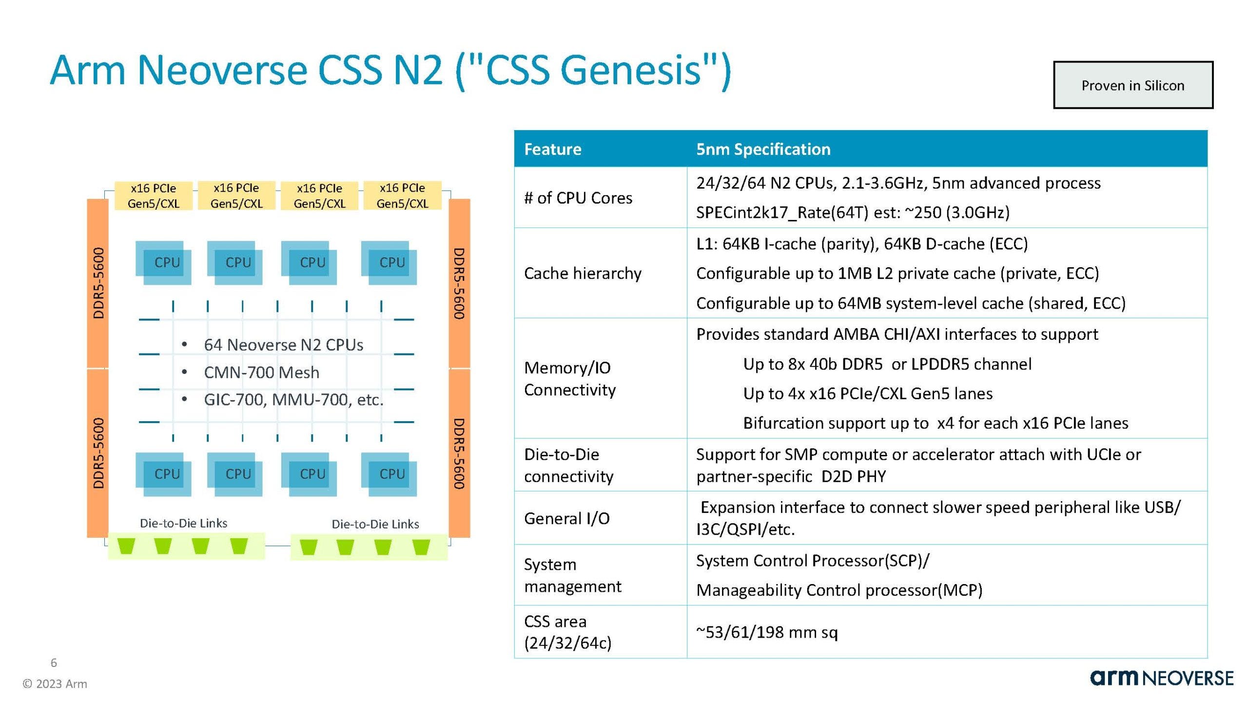
According to persistent industry chatter, the Cobalt 100 may be based on Arm’s very successful Neoverse Compute Subsystem (CSS) initiative, which was examined in detail here. Instead of simply offering the CPU core IP (and eventually its verified implementation in silicon for a popular process node), CSS allows Arm to offer its licensees almost the entire CPU design already validated in silicon and implemented as a RTL (to simplify, that is all what is necessary for a foundry to build the finished product).
In more detail, along with CPU core IP, the CSS provides almost all the uncore components. Namely:
· First and foremost, the CSS includes the Arm CMN 700, which is the Mesh Based Coherent Interconnect. It is the interconnect that binds together all the sub-blocks of the processor together, and it allows for memory coherency. It is extremely important in a big CPU, and can make or break a design.
· The System Control Processor (SCP) and the Manageability Control Processor (MCP). The SCP provides internal management of the entire processor while the MCP allows for communication with the external platform-level management controller (the BMC).
· The Memory Management Unit (MMU) and the Generic Interrupt Controller (GIC). The MMU is required to handle memory address translation and is basically required in all modern processors. The GIC handles interrupts and an equivalent controller is also found in every single processor.
· Various optional interconnect, like “Accelerator Attach” (to directly attach accelerators with custom interconnects, for performance purposes), “Multichip Interfaces” (to cobble together two dies in one package), and “CMN Gateway” for multi-socket interconnects.
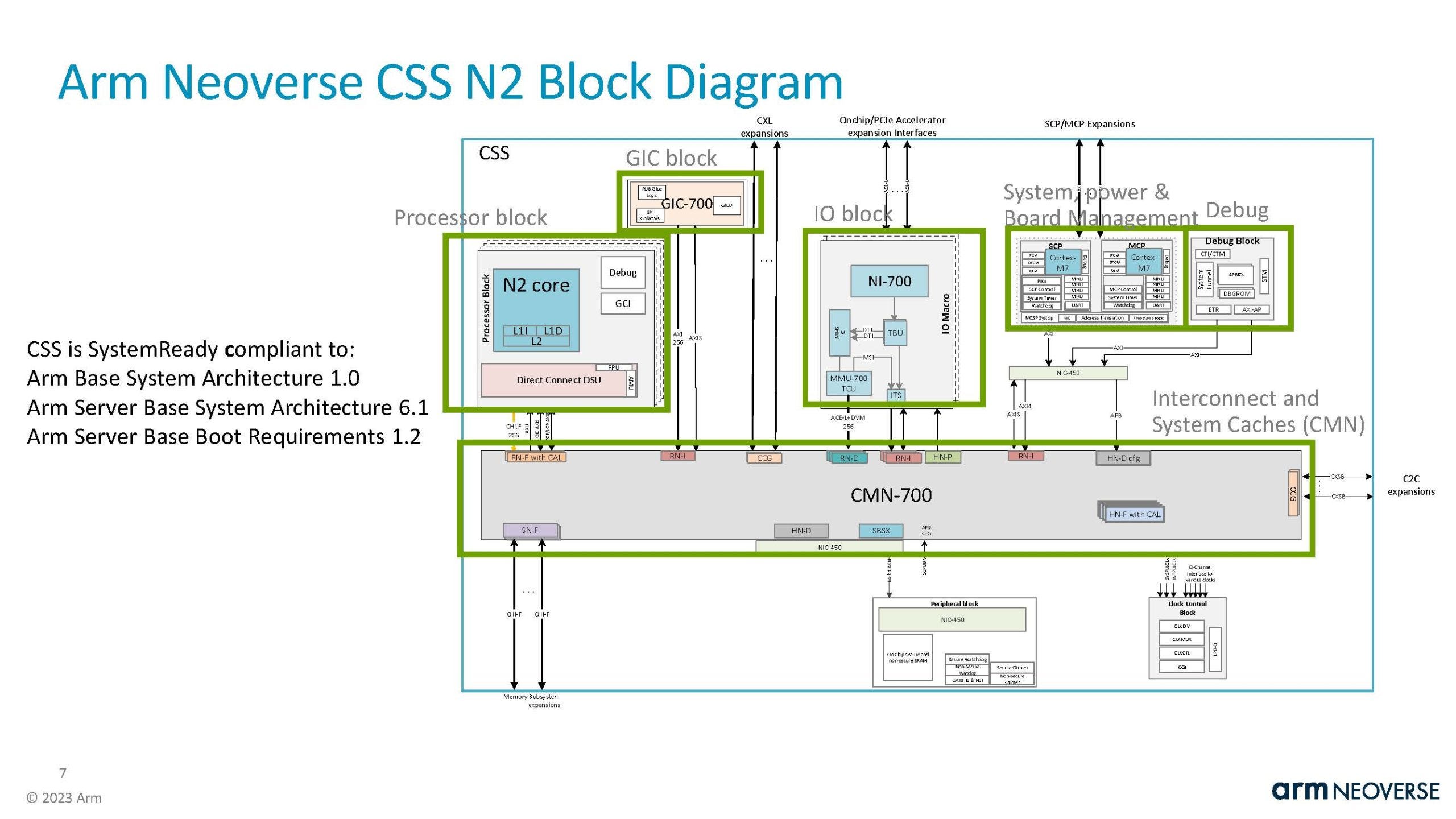
Not included in the CSS are the PCIe/CXL IP blocks and the memory controller IP blocks. It just so happens that the entire industry (except maybe for the likes of Intel and AMD, and possibly Apple and Qualcomm, that probably design their own PCIe and memory IP blocks) has settled a few years ago on the IP blocks offered by renowned IP giants Synopsys and Cadence for these sub-blocks, and Arm has stopped offering new versions of its memory controller IP blocks since the launch of the CMN 700 mesh interconnect in 2021.
Crucially all of these IP blocks are validated in silicon for a specific process node (in this case TSMC’s 5nm), which makes life incredibly easier for the Arm licensee.
Why bother with all these details, one may ask. Well, this shows that a modern server CPU is much more than just the implementation of the CPU core IP, and there are many other critical components that need to be developed, tested, and validated in silicon. With the CSS, Arm allows its licensees to experience a huge reduction in time to market, which is utterly important in this industry.
By implementing the 200 mm sq (a relatively modest die size for such a powerful chip) 64 cores variant of the N2 CSS, Microsoft may have been able to come up with a dual die, single package, 128 cores monster in a record 13 months, which is simply astonishing. The Arm CSS pushes the boundaries of the “off the shelf” concept even further, allowing a paradigm-shifting reduction in time-to-market. Please note that Arm’s CSS are only available for the N2, N3 and V3 cores, so none of the Graviton CPUs could have benefited from it.
A quick look at the Google’s Axion CPU and a table to recap it all
After AWS that started its trailblazing journey back in November 2018, and Microsoft that made its first announcement in November 2023, Google is the last of the big three Cloud Service Providers to announce its homegrown Arm datacenter CPU: the Google Axion. Almost nothing is publicly known about it, except that it is based on the Arm V2 CPU IP. One notable fact is that it incorporates the in-house Titanium controllers designed to off-load network and storage I/O processing and security operations.
This highlights one of the many advantages for the biggest CSPs to adopt self-designed hardware: they can tailor their hardware to their specific needs. This mostly relates to specific network and storage optimizations and hardware acceleration, just like AWS has been doing for many years with its homegrown Nitro DPU since at least 2021.
This way, CSPs can co-optimize their in-house software stack with their indigenous hardware, thus creating a virtuous circle of lower TCO and greater control over their critical supply chains. In other words, once they get a taste of it, and unless some of them hit a brick wall of repeated execution failures, it will be very hard to convince the biggest CSPs and hyperscalers to come back to commercial offerings. That would mean higher acquisition costs, higher operating costs (with no optimizations for the in-house software stack), and less control on the timing of hardware refresh cycles. Higher TCO and less overall control over the infrastructure buildout aren’t exactly great conversation starters in corporate boardrooms.
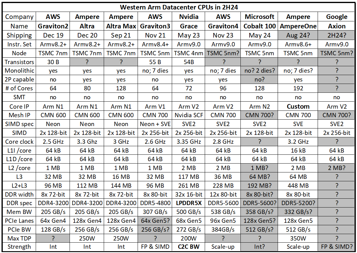
The following table recapitulates the specifications of the homegrown Arm datacenter CPUs of the three biggest Western Cloud Service Providers. Arm’s IP reigns supreme here, and that’s not by accident. Time to market, anyone? Please note that the greyed-out specifications for the Cobalt 100 assume that it is indeed based on a dual-die Arm CSS N2 implementation (see CSS slide above for more details). Also, no Graviton1 in this table as it is simply not relevant anymore.

Ampere Computing, the only Western commercial Arm Datacenter CPU player left
Beyond the CSPs indigenous efforts, and notwithstanding Nvidia’s special case which we will get to further below, Ampere Computing is indeed the last commercial Arm datacenter CPU maker left standing, after Marvell quit the market by cancelling its ThunderX3 line in August 2020. It is of course very important to note that, Marvell being Marvell, they didn’t exactly abandon this market, but rather redirected their ambitions towards building ASICs (including CPUs) for third parties. Together with Broadcom and lesser-known players like GUC, Marvell is indeed one of the few companies with the requisite know-how necessary to capitalize on the CSPs and hyperscalers thirst for in-house silicon by helping them design their homegrown CPUs and accelerators.
In other words, Marvell decided that it had more chance of making money by building custom CPUs for third parties rather than launching an entire line of commercially available SKUs. Which brings us back to Ampere Computing. The company was founded in 2018 by former Intel President Renée James with funding from the Carlyle Group, Arm and Oracle. Oracle, of course, is often considered to be in the top five biggest Western CSPs, and has been one of the first big Ampere customers.
Ampere was the first to market with a commercially available 64+ cores Arm datacenter CPU in December 2020, choosing the off-the-shelf Arm N1 CPU IP for its first generation of products, the 80 cores Ampere Altra. This was quickly followed in September 2021 by a 128 cores variant, the Ampere Altra Max, which was basically the same CPU with more cores and slightly less L3 (probably the keep the monolithic die size in check). Even though the Altra made for a good “cloud workloads all-rounder” CPU, the Altra Max was badly starved of L3 and memory bandwidth, and thus could only shine in a specific subset of CSP workloads. See here this excellent review for more details on this matter. In any case, at that time, Ampere had come up with a solid, attractive and timely offering that boded well for the company’s future. But then came…
The fateful choice of custom Arm cores and the bane of execution problems
In May 2022, the company announced its next generation product, the 5nm AmpereOne, sporting up to 192 cores. The bombshell, of course, was that these CPUs would sport custom Arm cores instead of using Arm’s off-the-shelf IP. We have examined the debate around “off-the-shelf vs custom cores” before, and four years later, not much has changed. The “off-the shelf strategy” is less risky (especially for a company with limited resources), and allows for shorter time-to-market (TTM). As for the “custom cores strategy”, let’s quote the piece published by STH four years ago:
“The custom cores strategy can only pay off if one is able to execute well enough and fast enough, all the while offering an obvious price or performance advantage. It necessitates a lot more resources, but if the differentiation is a win with customers, the payoff can potentially be big.”
The problem, of course, is that for all intents and purposes, AmpereOne is pretty late, and has only been shipping this month (August 2024). This may be viewed as a controversial statement, as AmpereOne’s availability in the cloud has been announced many times these past 18 months. However, trustworthy sources like Michel Larabel from Phoronix and Patrick Kennedy from Servethehome pretty much confirm that AmpereOne’s availability has been a pretty big problem. [August 2024 is probably the month when AmpereOne really becomes available. Expect third party benchmarks of AmpereOne *very* soon]
It is of course impossible to know if the delay incurred by AmpereOne is due to the choice of custom cores or to some other factors. It could be due to a separate design problem. But one thing is certain: opting for Arm’s off-the-shelf CPU IP allows for lower risk and faster time to market, all things that AmpereOne has sorely missed. From September 2021 to August 2024, this three years delay is the sign of a serious execution problem.
Yet another table, and Ampere’s future outlook
This table recapitulates all Western Arm datacenter CPUs available by 24H2. More about Nvidia’s Grace special case in the next chapter below.
One important note:
The “shipping” line indicates start of preview or beginning of significant volume deployment; yes, we are comparing apples and oranges here, and CSPs’ in-house CPUs and commercially available ones are different beasts altogether.
On the face of it, AmpereOne doesn’t look out of place, with a 192 cores 2P platform shipping *now*. But a closer look reveals a damaging three years delay between Altra Max and AmpereOne. Also, shipping an Armv8.6+ in 24H2 is not a good look when Armv9.0 designs have been coming out since mid-2023. Of course, not supporting Armv9.0 instructions may not be such a big deal for many CSPs, as most of them are probably more interested in maintaining a single software support baseline (Armv8.0), but it is nonetheless the unmistakable sign of a detrimental delay. It also shows that the “custom cores strategy” can be truly unforgiving when concurrent with execution problems.
These past few days (August 2024), Ampere has updated their roadmap, and it certainly makes sense. AmpereOne M is to AmpereOne what Altra Max was to Altra: a derivative design with only one significant update. This allows the company to stay relevant all the while reducing to a minimum the resources allocated to a new design. So, the AmpereOne M is an AmpereOne but with 12 DDR5 memory “channels” instead of 8. This will obviously require a new socket and new motherboards, but these will be made worth investing in by the future advent of AmpereOne MX, a 3nm 256 cores variant using this 12 “channels” platform. This 256 cores variant was announced three months ago. All of this is of course facilitated by the chiplet based design. The novelty here is a future 512 cores product including AI silicon for training and inference, and to be air-cooled.
The idea of running inference on CPUs – at least for some players in the industry – is nothing new and as been discussed at length for example by the excellent Timothy Prickett Morgan from nextplatform.com. Air-cooling, for its part, is certainly a must if you want your product to be successful in the market, as not every datacenter is ready for water-cooling, as shown for example in this great piece from Semianalysis about Nvidia’s Blackwell respin.
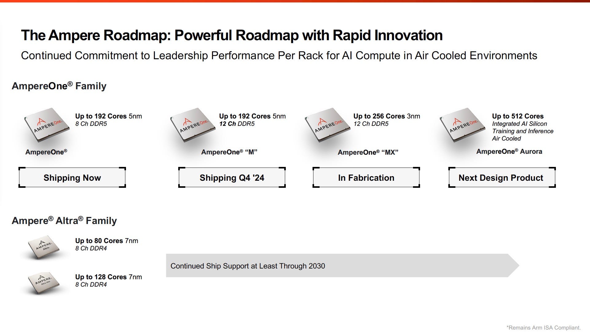
A roadmap is nice, but nobody can do compute on paper-launched products. Ampere Computing cannot afford another delay like what just happened with AmpereOne. Going for custom cores probably wasn’t a good idea. To Ampere’s defense, this decision was made a very long time ago – probably at least five years ago – long before the availability of Arm’s CCS IP allowed for incredibly short time-to-market (TTM). But even then, TTM was – and still is – everything in this market. Which customers care about the supposed advantages of cloud native custom Arm cores when the price to pay is a 12+ months delay, especially when Arm’s Neoverse lineup of CPU IP is considered good enough by every single hyperscaler out there?
And at the end of the day, the Carlyle Group isn’t in it for the glory, and will at some point in the future look for a ROI. So, after the AmpereOne family (AmpereOne, AmpereOne M and AmpereOne MX), don’t be surprised if the company pares down its initial custom cores ambitions and we all discover that AmpereOne Aurora adopts Arm off-the-shelf CPU IP. This is all speculation of course, and the future is uncertain. For now, let’s examine...
Nvidia Grace: a special case not designed to compete with traditional datacenter CPUs
There is one last Western Arm datacenter CPU to mention here: Nvidia’s Grace. This is however a special case, and isn’t meant to compete with the likes of Graviton4 or AmpereOne. This CPU is meant to be a companion to the company’s GPUs, and its standout feature is its dedicated interconnect to do just that, along with the enormous chip-to-chip (C2C) bandwidth that goes with it: 900GB/s. Grace can be directly linked to one or two Hopper or Blackwell GPUs, as shown here. Nvidia also offers what it calls the Grace Superchip, that is, two Grace CPU linked together with said C2C interconnect.
Notwithstanding the fact that Nvidia probably doesn’t want to sacrifice its high margin to try and compete in the market for Arm datacenter CPUs, there has been a few deployments of Grace-only configurations, but mostly by public research labs that also happen to have bought a lot of Nvidia’s GPUs. In other words, Grace-only deployments are pretty limited, and further restricted to buyers of Nvidia’s GPUs that probably managed to get a pretty good deal on price. This is especially true of public research labs, where Nvidia might be more than happy to lower its prices in pursuit of further cementing CUDA mind-share among influential software developers. Case in point: the Isambard 3 supercomputer at the University of Bristol.
Nvidia’s Grace memory subsystem also indicates that it wasn’t meant to compete in the broader datacenter CPU market: it uses soldered-on LPDDR5X instead of swappable DDR5 RDIMM modules that every datacenter customer would certainly prefer. This innovation makes a lot of sense for Nvidia, as memory capacity is pretty much a given in Grace typical deployment scenarios (that is, as a necessary companion taking care of mostly I/O operations while the GPUs are responsible for the true compute heavy lifting), and LPDDR5X allows for more memory bandwidth and less power at the same bus width compared to traditional DDR5.
Finally, contrary to what it had done in the past with the ill-fated “project Denver”, Nvidia has opted for off-the-shelf V2 CPU cores here, probably foregoing the damaging NIH syndrome in favor of faster time-to-market. The fact that it didn’t use Arm’s CMN IP for the mesh can certainly be explained by the fact that this IP simply couldn’t accommodate the enormous 900GB/s bandwidth of its C2C interface, as stated above. Hence the custom Nvidia “Scalable Fabric” (SCF) instead of the ubiquitous Arm CMN 700.
The x86 Empire strikes back, first with AMD’s Bergamo
Now that we have taken an exhaustive look at the current Arm datacenter CPU landscape, it is now time to finally investigate the response of the two x86 incumbents to this flurry of successful Arm designs. To be clear, this response doesn’t disappoint. AMD was the first to counter attack with the launch of Bergamo in July 2023. This isn’t entirely surprising as until the middle of this year, Intel was still very busy getting out of the hole it had dug itself into with its 10nm disaster on the manufacturing front, and with the very painful “pipe-flushing” of the older SPR and EMR CPUs on the design front.
Back to Bergamo, AMD’s original datacenter CPU chiplet architecture also facilitated its ability to offer a truly cloud native datacenter CPU option relatively easily and quickly. Whereas every single chiplet-based CSP CPU is organized around a big central compute die surrounded by memory and PCIe I/O dies, AMD’s datacenter CPUs are designed the other way around: a huge I/O die surrounded by small compute dies (that are reused for desktop and high-end laptop products).
So, to address the new emerging “cloud native” datacenter CPU market, all AMD had to do was to design a new small compute die for this precise purpose. It did so with the magic of higher transistor density allowed by lower frequency. Indeed, everything else being the same (process node used, IP being implemented), it is indeed possible to achieve much higher transistor density if you are ready to forgo the very high clocks normally achieved by traditional x86 CPUs.
It all comes together when you consider what a “cloud native” datacenter CPU really is: a CPU with a higher compute density (more cores per socket) at the cost of slightly less performant cores; if the cores are identical, it simply means their maximum frequency will be lower. Compared to a traditional datacenter CPU, a cloud native CPU simply has higher multi-thread performance per socket, at the cost of lower single-thread performance per core. In other words, more cores per socket but the cores are running at a lower frequency (assuming the cores are identical).
Believe it or not, and again, all other things being equal (process node used and IP being implemented), a very high frequency require that the transistors are – so to speak – given space to breathe, and that results in a lower overall transistor density. If you abandon high frequency, you can achieve higher density, even if implementing the same IP on the same process node. Back to AMD’s cloud native endeavor, whereas its “traditional” Zen4 compute die was designed to reach up to 5.7 GHz (on the desktop), its denser Zen4c cloud native compute die tops out at 3.1 GHz. Hence the fantastic density AMD was able to achieve with the Zen4c compute die:
16 Zen4 cores and 32 MB of L3 cache topping out at 3.1 GHz in 73 mm² sq for the Zen4c compute die versus
8 Zen4 cores and 32 MB of L3 cache topping out at 5.7 GHz in 66 mm² sq for the Zen4 compute die.
Zen4c: a density tour de force, together with AVX-512 and SMT
We are simplifying things a bit here, (single CCX in the Zen4 die vs dual CCX in the Zen4c die; no TSV in the Zen4c die; and the Zen4 die has logic to support 96 MB of L3 cache for the 3D V-Cache SKUs), but this is akin to almost doubling the compute density per compute die. However, AMD could only place 8 Zen4c compute dies on its SP5-based package versus 12 Zen4 compute dies for its more traditional offering, codenamed Genoa. Hence Bergamo only tops out at 128 cores per socket (8 73 mm² sq compute dies with 16 cores each; 8*16) while Genoa tops out at 96 cores (12 66 mm² sq compute dies with 8 cores each; 12*8). This discrepancy will be carried over to the Zen5 generation, with the “normal” Turin sporting 16 Zen5 compute dies with 8 cores each (128 cores in total), while Turin dense, the successor to Bergamo, will sport 12 Zen5c compute dies with 16 cores each (192 cores in total).
However, whereas the Zen4 and Zen4c compute dies were implemented on the same process node (TSMC 5nm), the situation will change with Zen5. While the “normal” Zen5 compute die will use TSMC 4nm node (a refined 5nm node), the Zen5c compute die will use TSMC’s brand new N3E (3nm) process node. This is mostly due to TSMC’s decision to change course on its 3nm family of nodes mid-journey after its first iteration (N3B) was deemed too costly, and AMD’s decision to edge their bets by porting Zen5 to 4nm, all the while choosing N3E for the much denser Zen5c. But this is a story for another day.
Back to the matter at hand, the beauty of the Zen4c cores is that they are exactly the same as the Zen4 cores, simply running at a lower frequency. This allows AMD to save on precious engineering resources by not developing a distinct CPU architecture for the cloud native market, all the while offering bonus features like SMT and AVX-512. Truthfully, SMT (simultaneous multi-threading) and AVX-512 are not exactly the first things a CSP is looking for in a datacenter CPU. As we have seen in the previous tables, no Arm processor described above supports SMT, and for good reasons: a CSP’s job is to run its customers workloads, and SMT can introduce the noisy neighbor effect, or – worse still – potentially nefarious interactions between the workloads of two different customers running on the same core. AVX-512, for its part, is only useful for a very specific subset of workloads, and require a software rewrite to be taken advantage of. But at the end of the day, both SMT and AVX-512 basically come for free in AMD’s cloud native offerings and can be disabled/discarded very easily with zero drawback. So, count this as a clear win for AMD, especially compared to…
Intel’s Sierra Forest, the Return of the King
There is *a lot* to say about Intel, about how it dug itself into a hole this last decade, and about how it is now trying to get out. See here for our first part on Intel’s odyssey to Hell and back. Expect the second part before the end of August 2024. In any case, Sierra Forest is the first part out of the company bearing the mark of a true renewal initiated by its new CEO, the Bible quoting Pat Gelsinger. And in fact, 2024 is truly the year when the new Intel will be getting out of excuses, as the “pipe-flushing” era of Meteor Lake, Sapphire Rapids and Emerald Rapids is now truly over, and the new CEO won’t be able to say something along the lines of: “Yes, these parts are underperforming, but it’s not my fault, as they were already well into the design phase when I came onboard!” Furthermore, it is important to distinguish between Intel’s efforts on the design front, competing against the likes of AMD and Nvidia, and its efforts on the manufacturing front, competing against TSMC. Yes, these are two very different kinds of ventures. Four years ago, Intel could already be seen as the last dinosaur, not having gone fabless (if you are ready to count Samsung as a special case due to its huge memory manufacturing operations). Nowadays, with TSMC utterly dominating the leading-edge foundry game in terms of technology (packaging included), volume and breadth of customers, Intel really looks like an out-of-place company in an entirely fabless world. So don’t be surprised if the Santa Clara company ends up spinning-off its fabs in a few years, once it is able to credibly reclaim the technological crown on the foundry front with the advent of its 18A process node.
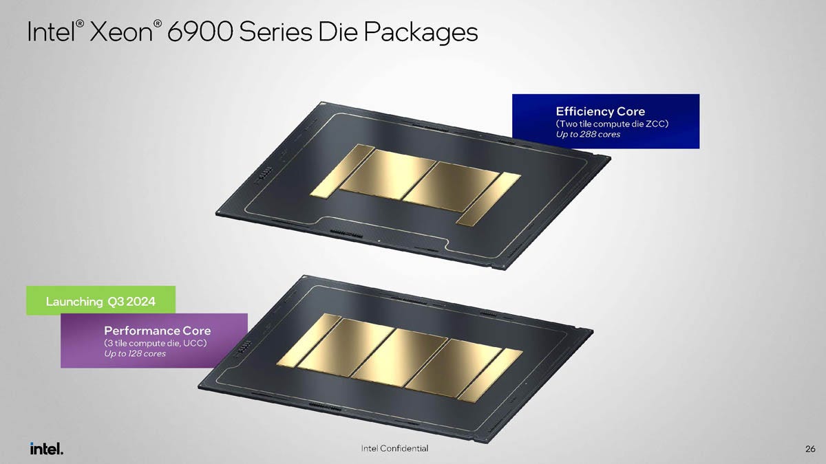
Back to Sierra Forest (SRF), it is an interesting beast, built in truly unique way. But to better understand this, we will have to take a look at Intel’s entire 2024 server offerings. There will be basically two distinct lineups: the cloud native Sierra Forest (E-cores), and the traditional, higher performance Granite Rapids (P-cores). Each of these two will be implemented on two distinct but common platforms: a 12 DDR5 “channels” platform (Xeon 6900), and an 8 DDR5 “channels” platform (Xeon 6700). Yes, this is a common theme in the industry, as Ampere is doing the same with AmpereOne and AmpereOne M (see above), and so is AMD with its 12 “channels” SP5 socket for Genoa and Bergamo and its 6 “channels” SP6 socket for more reasonably sized products codenamed Siena (not detailed here for simplicity’s sake). Basically, all manufacturers of commercially available datacenter CPUs are trying to balance the need to pass through the memory wall, which requires more memory channels, with the need to keep total platform costs in check for customers with lower compute requirements, hence the availability of variants with only 8 or 6 DDR5 memory “channels”.
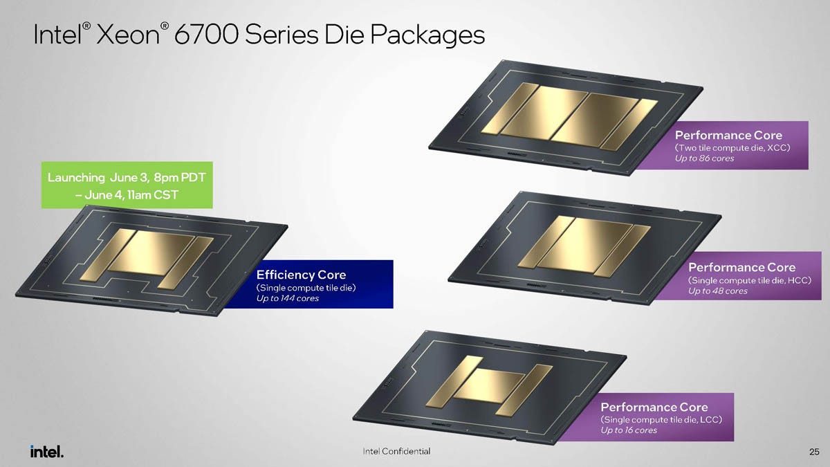
As we are comparing x86 and Arm datacenter CPUs here, we will limit ourselves to Intel’s cloud native lineup, based on what the company calls its Efficiency Cores (E-cores). But just to be clear, Sierra Forest (E-cores) is to Granite Rapids (P-cores) what Bergamo was to Genoa, and what Turin-dense will be to Turin: the new cloud native lineups from the x86 incumbents, offering more compute per socket at the cost of lower single-thread performance per core, because this is exactly what the CSPs of this world want: more compute density, even at the cost of lower single-thread performance. As of August 2024, Intel has only launched the 8 “channels” variant of Sierra Forest; that’s the Xeon 6700E in Intel parlance: “6700” for the 8 “channels” platform, and “E” for the cloud native SKUs.
Compared to the in-house designs of the CSPs (a big single compute die surrounded by small I/O dies) and to what AMD has done since Zen2 (a big single I/O die surrounded by small compute dies), Intel has opted for a third way for Sierra Forest (SRF) and Granite Rapids (GNR). These CPUs have huge compute dies that incorporate memory controllers, surrounded on each side by PCIe/CXL I/O dies that are shared between these two platforms. Hence the Xeon 6700E (SRF 8ch) has a single 144 cores compute die, whereas the future Xeon 6900E (SRF 12ch) will incorporates two 144 cores compute dies, toping out at 288 cores with 12 memory “channels”. The advantage here is that the memory controllers are “on die”, that is, on the same die as the compute units, which allows for lower latency and thus higher performance. In more details, the 144 cores SRF compute die incorporates an 8 DDR5 “channels” memory controller. The dual die 288 cores beast will be able to control in total 16 (2*8) DDR5 “channels”, only 12 of which will be used. The drawback, of course, is that these dies are pretty big, and will thus be relatively expensive to manufacture. However, and that’s what’s truly remarkable with Sierra Forest and Granite Rapids, these CPUs are manufactured on Intel’s new 3nm process node, called “Intel 3”. After the terrible fiasco of Intel 10nm process node (that was at some point renamed Intel 7, to better reflect its real density compared to TSMC’s offerings and to better hide the company’s defeat on the manufacturing front), Intel’s 3nm process node is the first competitive node coming out of the company since the glory days of the 14nm era! For exhaustivity’s sake, Intel 4 was just a de-risking step on the road to Intel 3, only used by Intel itself, and only a few libraries were ported to that node; Intel 3 however, will be used by third party customers, and Intel will port all the libraries that it can to it.
That is why Sierra Forrest marks the true return of Intel to the datacenter CPU market: for all intent and purposes, it is a very competitive cloud native offering, with outstanding power efficiency (which is the one thing CSPs care about, as a better power efficiency leads to a lower TCO), and being implemented on a competitive in-house process node, which allows Intel to avoid the TSMC tax and to preserve its margins on these products.
The Pros and Cons of a distinct microarchitecture
The other big difference between Intel’s Sierra Forest and AMD’s Bergamo (and the future Turin-dense), is that Intel uses an entirely different microarchitecture for its cloud native lineup. This microarchitecture is the direct descendant to the Intel Atom line of CPUs, which first debuted in 2008. Over the course of 16 years, it has known many iterations. After first being used exclusively in ultra low power, ultra cheap notebooks, its focus was then enlarged to CPUs designed for micro server applications, starting in 2013 with the very successful Avoton/Rangeley lineup. And in 2021, Intel implemented for the first time the newest version of its low power Atom microarchitecture (now called E-cores) on its highest performing process node, pushing these low power cores to very high frequency compared to previous generations (up to 3.9 GHz instead of 2.4 GHz previously). All in all, from Bonnell to Cresmont, there have been 8 iterations of the Atom line of CPU cores, and starting from Gracemont and then Crestmont, these cores have nothing to be ashamed of anymore in terms of single-thread performance, all the while maintaining very high power efficiency and “transistor efficiency” (they are small). In other words, Intel has figured out the PPA conundrum with Cresmont, and that is why it makes for such a great cloud native CPU.
However, this has two main drawbacks for the Santa Clara company: the lack of SMT support, and the lack of AVX-512 support. And even if, as stated above, these features are not exactly “must haves” in the realm of cloud native CPUs, not having them can be viewed as a relatively important disadvantage for Intel when compared to AMD’s Zen4c and Zen5c offerings.
One last table to rule them all and closing thoughts

Hopefully, after this pretty long exposé, the reader has a better view of the landscape of cloud native CPUs. Three main categories emerge:
· The three biggest CSPs, which can achieve lower TCO and better control over their supply chains with their in-house Arm CPU designs. Just like Apple, it will probably be very hard to convince them to come back to commercial offerings, as they have enough volume to justify the cost associated with in-house silicon development. AWS is way ahead of Microsoft and Google in this regard.
· Ampere Computing, the only company left offering commercial Arm datacenter CPUs. With its choice of custom Arm cores, it may have designed itself into a corner, especially in terms of time to market. AmpereOne is late, and once they became available, it is probably not entirely unreasonable to expect third party benchmarks to be at least somewhat underwhelming. However, Ampere has this market basically all for itself, so its future may be safe if it can avoid any future execution problems.
· The two x86 incumbents, Intel and AMD. They aren’t sitting idle either, and have identified the threat of Arm datacenter CPUs long ago (these things take years to design). Since Zen2, AMD has become a pretty agile player in the datacenter CPU market thanks to its very innovative chiplet-based design, and Zen4c is definitely a design tour de force.
· Notwithstanding the “noise” around its very disappointing 2Q24 financial results, Intel is back, with a truly competitive cloud native CPU offering (for the first time since 2019) implemented on a truly competitive in house process node, Intel 3. This is a good sign for Gelsinger’s turnaround, but the road will be long and hard.
· Time to market (TTM) is of paramount importance here.
· Arm’s CSS IP has reached the perfect sweet spot between TTM accelerant and customizability for customers, and will certainly continue being successful in the future.
· If Ampere Computing really doesn’t manage to right itself, much more powerful players like Qualcomm or Nvidia may decide to enter the fray.